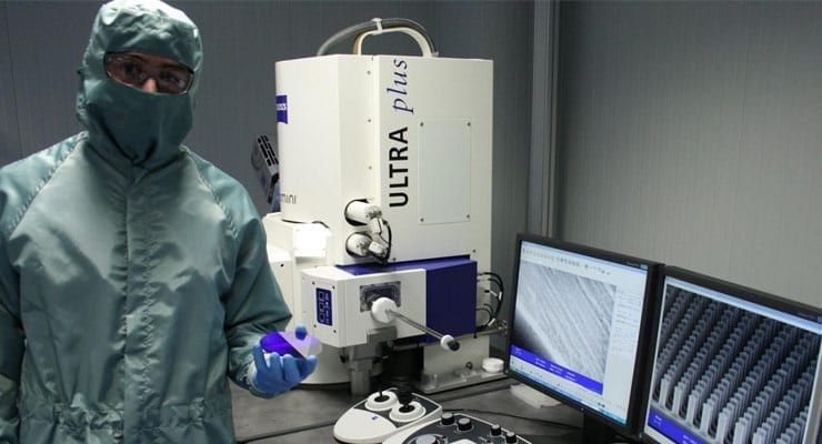
The industry of semi-conductor materials is helping to dramatically progress micro- and nano-fabrication techniques, facilitating increasingly smaller components that are closer to each other.
Within the techniques used in these processes, one research team led by Iñaki Cornago at the Universidad Pública de Navarra has made use of what is known as laser interference lithography, which consists of applying laser radiation to a photo-sensitive material to create structures on a nanometric scale.
In this case, he used glass, gold and silicon, among other materials, to which he gave shapes such as lines, holes, pillars or cones.
The applications of these nanostructures can be classified in two groups: biosensors and anti-reflective surfaces. The nanostructures are used to obtain an optical response to a biological reaction, allowing information to be obtained about the presence of a substance in a sample.
The thesis, supervised by Rafael Rodríguez-Trías, lecturer in the NUP/UPNA’s Department of Mechanical, Energy and Materials Engineering, and the PhD holder in Engineering Javier Bravo Larrea, presents a range of biosensor types that can be used in the biomedical sector to detect diseases in biological samples, such as blood or urine; or in the environmental sector to spot toxins or chemical contaminants in marine waters.
Antireflective applications of the nanostructures can improve public safety or give a boost solar energy. “This mechanism can be used to minimize, for example, the undesired reflections that are produced in glasses, windows or car windows and also the reflection produced on solar panels, which can increase the efficiency of these photovoltaic cells,” said Cornago.


